InfraScopeTM MWIR Temperature Mapping Microscope:
InfraScopeTM Temperature Mapping Microscope addresses an important aspect of managing device reliability. True temperature mapping supplies data critical to the reliability and thermal management concerns of semiconductor engineers working in Design, Packaging, Reliability, Microwave, RF, MEMs, and other areas.
QFI temperature mapping software performs automated emissivity correction to produce a true temperature map with high temperature and spatial resolution. Movie mode is used for testing time varying effects. The InfraScopeTM 2D MWIR Temperature Mapping Microscopy solution has been used to verify thermal design rules, verify die and solder attachment, localize reliability issues and optimize thermal packages. Temperature mapping functions for both front and backside inspection. Given that the wavelengths involved are infrared, the custom microscope objectives are made with infrared transmissive materials such as silicon, germanium, sapphire and zinc selenide.
Most of the contrast in an unprocessed infrared image of a circuit is NOT due to temperature. Rather, in an unprocessed image, differences in emissivity create the most contrast. Emissivity is a material property that influences how efficiently the material emits photons. QFI uses patented algorithms and proprietary software to measure and compensate for the emissivity of the material being tested in order to generate an accurate, calibrated temperature map image. Pixel-by-pixel emissivity measurement and compensation has been practiced on QFI systems for many years. QFI’s solution is rapid, accurate and automatic.
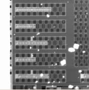
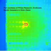
The 5x magnification backside images below are from a sample provided by Philips Research, Eindhoven, through the courtesy of Martijn Goossens and Victor Zieren. The sample is decapsulated on both sides. The process is six-metal-layer (copper), on a 10 Ohm.cm p-epi silicon substrate, thinned to 102 um.
The Details
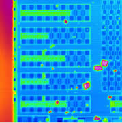
Details A – Radiance image captured on unbiased/unpowered device at elevated temperature evidences emissivity variations of different materials in the semiconductor device.
Details B – QFI manufactures thermal stages to enable temperature control of wafers and packaged IC components. Using patented and proprietary algorithms, a pixel-by-pixel emissivity correction map is calculated for the device. QFI has multiple emissivity correction methods.
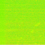
Details C – After emissivity correction, an image of the unbiased device at any temperature will show a uniform temperature map.
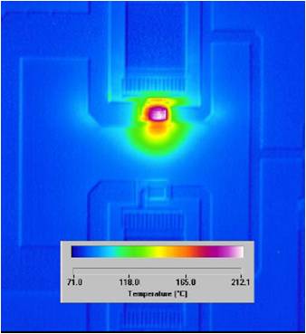
Details D – Post emissivity correction, the InfrascopeTM will capture an accurate, calibrated temperature map of the DUT.
The user easily determines the precise temperature at any point by color or by simply positioning the mouse arrow over the desired point and reading the desired temperature. This technique saves literally hundreds of hours over non-infrared techniques and it doesn’t damage or affect the part in any way.
You are welcome to request additional information via the information request link:

